Advances and Applications of 2D Materials in Technology
This review looks at the synthesis, characteristics, and uses of 2D materials, emphasizing their disruptive potential in technology and providing insights into future research and development prospects.
Introduction to 2D Materials
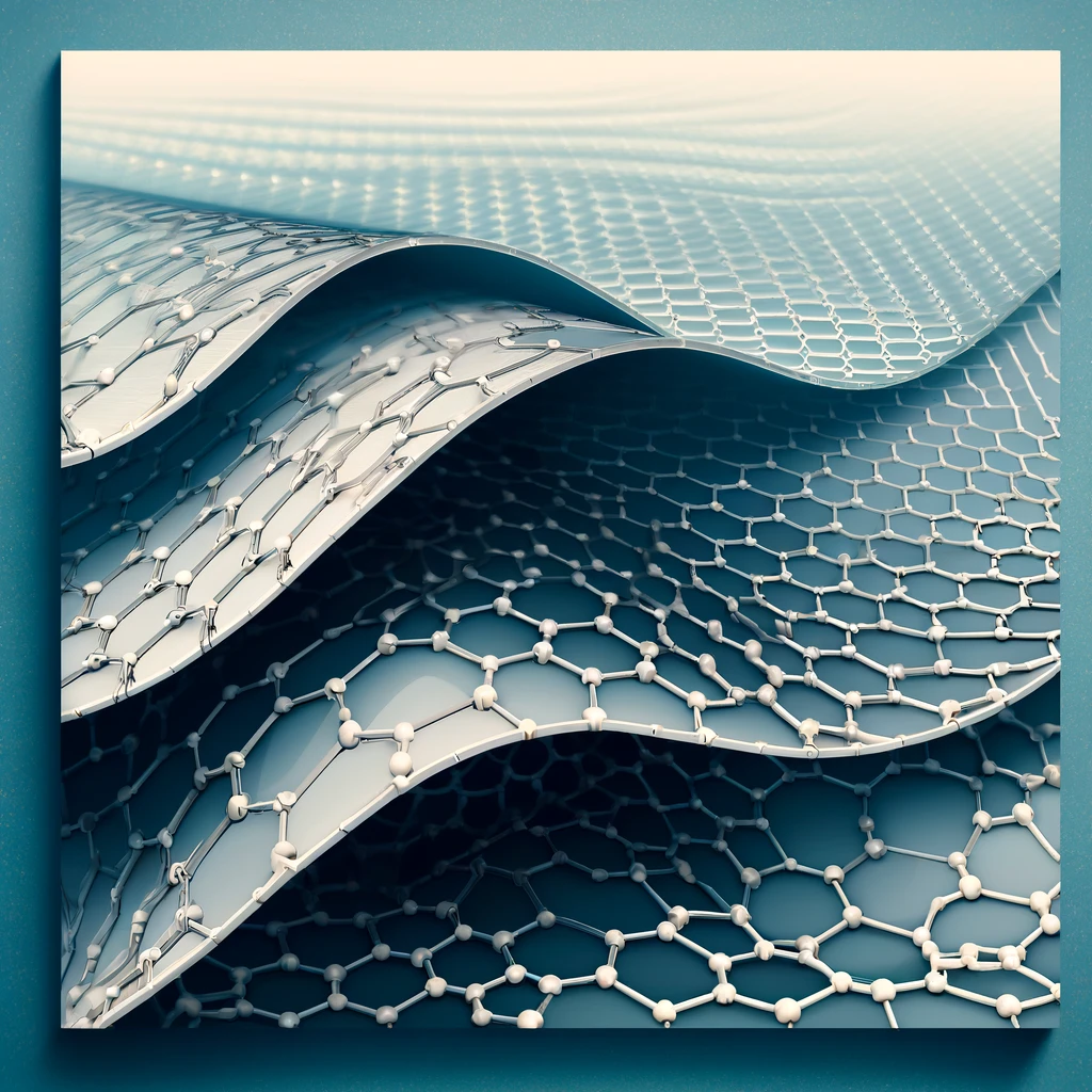
The phrase “2D materials” refers to bulk materials with a layered structure and van der Waals (vdW) force interaction between layers (Wei et al., 2019). These materials feature atomically thin structures, which make it possible for researchers to engineer and adapt their characteristics, such as bandgap, surface and edge reactivity, and electronic and optoelectronic capabilities, into distinct physical properties (Nayir et al., 2023). 2D materials have unique layered properties that are devoid of surface connections, and their atomically flat surfaces make them appealing for nanoelectronic applications (Lee et al., 2019). The discovery and historical development of 2D materials has been significantly accelerated by the creation of databases containing a large number of 2D materials with calculated fundamental properties, which are then intelligently mined for materials with desired properties for specific applications. Compositing 2D materials with other materials can improve their electrochemical properties and reduce flaws (Xiao et al., 2021).
The computational 2D materials database provides a comprehensive and easily accessible overview of the continuously expanding family of 2D materials, serving as an ideal platform for computational modeling and creation of new 2D materials and van der Waals heterostructures (Haastrup et al., 2018). Two-dimensional (2D) materials are ideal for next-generation electronics due to their unique physical, optical, and electric properties, such as atomically thin bodies, high transmittance, ultralight weight, and tunable band structures (Ricciardulli & Blom, 2020). The development of novel 2D materials with superior electrical and optoelectronic capabilities has sparked widespread scientific interest (Qiao et al., 2022). Furthermore, the fabrication of “true” 2D materials has recently received a lot of attention in the search for new functional materials with unparalleled properties (Xu et al., 2014).
2D materials are commonly employed in optical and photonic applications such as mode locks, optical switches, polarizers, and optical modulators (Liu, 2023). The discovery of 2D intrinsic magnetic materials with ultrathin structures and smooth surfaces has enabled research into fundamental magnetism physics and the development of spintronic devices (Hao et al., 2022). Two-dimensional (2D) layered materials have arisen as a new platform for conducting innovative electronic, optical, or excitonic physics and developing unparalleled nanoelectronic and energy applications (Chen et al., 2018).
Synthesis and Characterization
Salt-templating, molten Lewis acid etching, chalcogen vapor etching, and chemical vapor deposition (CVD) are some of the processes used to synthesize 2D materials (Kim et al., 2021; Geng and Yang, 2018; Dong et al., 2021). Beyond graphene and transition metal dichalcogenides, these approaches allow for the controlled creation of 2D materials such as transition metal chalcogenide. Photoexfoliation and epitaxial growth on SiC are also used to synthesize 2D materials (Kumar et al., 2022; Li et al., 2017).
Pressure bulge testing for mechanical properties (Cao & An, 2023), thermal characterization techniques including optothermal Raman and micro-bridge methods (Liu et al., 2021), and electrical characterization using field-effect transistors (Mitta et al., 2020) are all used to characterize the physical and chemical properties of 2D materials. The structural characteristics of 2D materials are characterized using optical inspection techniques such as optical microscopy (Lee et al., 2021). Additionally, epitaxial growth methods and controllability are investigated for the scalability of 2D layered transition-metal dichalcogenides (Li et al., 2017).
2D materials are synthesized using a variety of methods, including salt-templating, etching, and CVD, and their physical and chemical properties are characterized using techniques such as pressure bulge testing, thermal characterization, electrical characterization, and optical inspection.
Applications and Future Prospects
Current applications for 2D materials include electronics, energy storage, and biomedicine. In electronics, 2D materials have showed potential in optoelectronics, innovative electronics, and as building blocks for integrated electronic and optoelectronic devices. Preischl et al. (2020). Chen et al. (2018), Li et al. (2017), Anam & Gaston (2021), Yu & Yang (2020), Schmid (2024), Tian et al. (2018), Sun & Wu (2018), Xie et al. (2021), Rafieerad et al. (2021), Mojtabavi et al. (2021), Miao et al. (2023), and Liu et al. (2022). 2D materials have been used in electrochemical energy storage devices, such as lithium-ion batteries and supercapacitors, due to their excellent electrochemical performance and high specific capacitance (Chen et al., 2018; Li et al., 2017; Anam & Gaston, 2021; Yu & Yang, 2020; Sun & Wu, 2018; Mojtabavi et al., 2021; Miao et al., 2023; Zhao, 2024; Katiyar, 2023; Batool et al., 2023; Kharwar et al., 2023; Qu Furthermore, 2D materials have found applications in biomedicine, including in nanomedicine and biomedicine, where they have been explored for potential applications in drug delivery, biosensing, and tissue engineering (Yu & Yang, 2020; Schmid, 2024; Tian et al., 2018; Sun & Wu, 2018; Xie et al., 2021; Rafieerad et al., 2021; Mojtabavi et al., 2021; Miao et al., 2023; Liu et al., 2022; Zhao, 2024; Katiyar, 2023; Batool
Future research paths and prospective technical improvements in the field of 2D materials are centered on a variety of topics. These include the creation of 2D materials for flexible electronics, which have the potential to give novel solutions to issues in a variety of electronic domains (Katiyar, 2023). Furthermore, advancements in 2D nanopatterning technologies are critical for producing high-quality material structures with ultrahigh integration density for future electrical and optoelectronic applications (Liu et al., 2022). Furthermore, the role of 2D materials in the creation of next-generation electronic devices with high performance, low power consumption, and high integration is being investigated, including non-volatile memory, Fe-FET, and neural network calculating devices (Zhang & Peng, 2023). The study of interfacial energy storage mechanisms is predicted to result in the development of energy storage devices with high energy density and power density (Hu et al., 2020). Furthermore, the potential of 2D materials in photonics and the energy storage business is being examined, with a particular emphasis on recent theoretical and practical advances (Iqbal et al., 2022). In biomedicine, 2D materials for nanoultrasonic biomedicine applications, such as high-intensity focused ultrasound (HIFU) and low-intensity sonodynamic treatment (SDT), are being developed (Tang et al., 2016).
To summarize, 2D materials have already found numerous uses in electronics, energy storage, and healthcare, and ongoing research is aimed at expanding their potential in these sectors. Future applications for 2D materials include flexible electronics, high-performance electronic devices, interfacial energy storage mechanisms, photonics, and nanoultrasonic biomedicine.
Reference
Chen, Y., Chen, C., Kealhofer, R., Liu, H., Yuan, Z., Jiang, L., … & Wu, J. (2018). Black arsenic: a layered semiconductor with extreme in‐plane anisotropy. Advanced Materials, 30(30). https://doi.org/10.1002/adma.201800754
Haastrup, S., Strange, M., Pandey, M., Deilmann, T., Schmidt, P., Hinsche, N., … & Thygesen, K. (2018). The computational 2d materials database: high-throughput modeling and discovery of atomically thin crystals. 2d Materials, 5(4), 042002. https://doi.org/10.1088/2053-1583/aacfc1
Hao, Q., Dai, H., Cai, M., Chen, X., Xing, Y., Chen, H., … & Han, J. (2022). 2d magnetic heterostructures and emergent spintronic devices. Advanced Electronic Materials, 8(11). https://doi.org/10.1002/aelm.202200164
Lee, K., Yang, S., Sung, Y., Chang, Y., Lin, C., Feng, Y., … & Lin, Y. (2019). Analog circuit applications based on all‐2d ambipolar rese2 field‐effect transistors. Advanced Functional Materials, 29(22). https://doi.org/10.1002/adfm.201809011
Liu, G. (2023). Emerging 2d materials with nonparabolic bands for ultrafast photonics. Small Science, 3(10). https://doi.org/10.1002/smsc.202300030
Nayir, N., Mao, Q., Wang, T., Kowalik, M., Zhang, Y., Wang, M., … & Duin, A. (2023). Modeling and simulations for 2d materials: a reaxff perspective. 2d Materials, 10(3), 032002. https://doi.org/10.1088/2053-1583/acd7fd
Qiao, Y., Shen, H., Zhang, F., Liu, S., & Yin, H. (2022). W4pcl11monolayer: an unexplored 2d material with moderate direct bandgap and strong visible-light absorption for highly efficient solar cells. Nanoscale, 14(34), 12386-12394. https://doi.org/10.1039/d2nr03009h
Ricciardulli, A. and Blom, P. (2020). Solution‐processable 2d materials applied in light‐emitting diodes and solar cells. Advanced Materials Technologies, 5(8). https://doi.org/10.1002/admt.201900972
Shen, L., Zhou, J., Yang, T., Yang, M., & Feng, Y. (2022). High-throughput computational discovery and intelligent design of two-dimensional functional materials for various applications. Accounts of Materials Research, 3(6), 572-583. https://doi.org/10.1021/accountsmr.1c00246
Wei, Q., Li, R., Lin, C., Han, A., Nie, A., Li, Y., … & Huang, W. (2019). Quasi-two-dimensional se-terminated bismuth oxychalcogenide (bi2o2se). Acs Nano, 13(11), 13439-13444. https://doi.org/10.1021/acsnano.9b07000
Xiao, Z., Wang, R., Jiang, D., Qian, Z., Li, Y., Yang, K., … & Wu, F. (2021). Recent developments of two-dimensional anode materials and their composites in lithium-ion batteries. Acs Applied Energy Materials, 4(8), 7440-7461. https://doi.org/10.1021/acsaem.1c01259
Xu, L., Zhou, X., Wang, T., Gao, T., Zhang, Y., Lei, S., … & Liu, Z. (2014). Surface‐confined single‐layer covalent organic framework on single‐layer graphene grown on copper foil. Angewandte Chemie, 126(36), 9718-9722. https://doi.org/10.1002/ange.201400273
Cao, G. and An, F. (2023). Mechanical properties characterization of 2d materials via pressure bulge testing. Journal of Physics D Applied Physics, 56(7), 075302. https://doi.org/10.1088/1361-6463/acadeb
Dong, J., Zhang, L., Wu, B., Ding, F., & Liu, Y. (2021). Theoretical study of chemical vapor deposition synthesis of graphene and beyond: challenges and perspectives. The Journal of Physical Chemistry Letters, 12(33), 7942-7963. https://doi.org/10.1021/acs.jpclett.1c02316
Geng, D. and Yang, H. (2018). Recent advances in growth of novel 2d materials: beyond graphene and transition metal dichalcogenides. Advanced Materials, 30(45). https://doi.org/10.1002/adma.201800865
Kim, Y., Woo, W., Kim, D., Lee, S., Chung, S., Park, J., … & Kim, H. (2021). Atomic‐layer‐deposition‐based 2d transition metal chalcogenides: synthesis, modulation, and applications. Advanced Materials, 33(47). https://doi.org/10.1002/adma.202005907
Kumar, P., Dey, A., Roques, J., Assaud, L., Franger, S., Parida, P., … & Biju, V. (2022). Photoexfoliation synthesis of 2d materials. Acs Materials Letters, 4(2), 263-270. https://doi.org/10.1021/acsmaterialslett.1c00651
Lee, Y., Chang, S., Chen, S., Chen, S., & Chen, H. (2021). Optical inspection of 2d materials: from mechanical exfoliation to wafer‐scale growth and beyond. Advanced Science, 9(1). https://doi.org/10.1002/advs.202102128
Li, H., Liu, Y., Aljarb, A., Shi, Y., & Li, L. (2017). Epitaxial growth of two-dimensional layered transition-metal dichalcogenides: growth mechanism, controllability, and scalability. Chemical Reviews, 118(13), 6134-6150. https://doi.org/10.1021/acs.chemrev.7b00212
Liu, J., Li, P., & Zheng, H. (2021). Review on techniques for thermal characterization of graphene and related 2d materials. Nanomaterials, 11(11), 2787. https://doi.org/10.3390/nano11112787
Mitta, S., Choi, M., Nipane, A., Ali, F., Kim, C., Teherani, J., … & Yoo, W. (2020). Electrical characterization of 2d materials-based field-effect transistors. 2d Materials, 8(1), 012002. https://doi.org/10.1088/2053-1583/abc187
Anam, B. and Gaston, N. (2021). Structural, thermal, and electronic properties of two‐dimensional gallium oxide (β‐ga2o3) from first‐principles design. Chemphyschem, 22(22), 2362-2370. https://doi.org/10.1002/cphc.202100267
Batool, S., Idrees, M., Han, S., Roy, V., & Zhou, Y. (2023). Electrical contacts with 2d materials: current developments and future prospects. Small, 19(12). https://doi.org/10.1002/smll.202206550
Chen, C., Xie, X., Anasori, B., Sarycheva, A., Makaryan, T., Zhao, M., … & Gogotsi, Y. (2018). Mos2‐on‐mxene heterostructures as highly reversible anode materials for lithium‐ion batteries. Angewandte Chemie, 57(7), 1846-1850. https://doi.org/10.1002/anie.201710616
Ciocys, S., Maksimovic, N., Analytis, J., & Lanzara, A. (2022). Driving ultrafast spin and energy modulation in quantum well states via photo-induced electric fields. NPJ Quantum Materials, 7(1). https://doi.org/10.1038/s41535-022-00490-2
Döscher, H., Schmaltz, T., Neef, C., Thielmann, A., & Reiß, T. (2021). Graphene roadmap briefs (no. 2): industrialization status and prospects 2020. 2d Materials, 8(2), 022005. https://doi.org/10.1088/2053-1583/abddcd
Hu, Y., Li, Y., Cheng, J., Chen, M., Fu, W., Liu, B., … & Shen, Z. (2020). Intercalation of carbon nanosheet into layered tio2 grain for highly interfacial lithium storage. Acs Applied Materials & Interfaces, 12(19), 21709-21719. https://doi.org/10.1021/acsami.0c03775
Iqbal, M., Malik, M., Shahid, W., Ahmad, W., Min-Dianey, K., & Pham, P. (2022). Plasmonic 2d materials: overview, advancements, future prospects and functional applications.. https://doi.org/10.5772/intechopen.101580
Katiyar, A. (2023). 2d materials in flexible electronics: recent advances and future prospectives. Chemical Reviews, 124(2), 318-419. https://doi.org/10.1021/acs.chemrev.3c00302
Kharwar, S., Singh, S., & Kaushik, B. (2023). Hydrogenated cove-edge aluminum nitride nanoribbons for ultrascaled resonant tunneling diode applications: a computational dft study. Nanotechnology, 34(24), 245709. https://doi.org/10.1088/1361-6528/acc035
Li, B., Gu, P., Feng, Y., Zhang, G., Huang, K., Xue, H., … & Pang, H. (2017). Ultrathin nickel–cobalt phosphate 2d nanosheets for electrochemical energy storage under aqueous/solid‐state electrolyte. Advanced Functional Materials, 27(12). https://doi.org/10.1002/adfm.201605784
Liu, S., Wang, J., Shao, J., Ouyang, D., Zhang, W., Liu, S., … & Zhai, T. (2022). Nanopatterning technologies of 2d materials for integrated electronic and optoelectronic devices. Advanced Materials, 34(52). https://doi.org/10.1002/adma.202200734
Miao, N., Gong, Y., Zhang, H., Shen, Q., Yang, R., Zhou, J., … & Wang, J. (2023). Discovery of two‐dimensional hexagonal mbene hfbo and exploration on its potential for lithium‐ion storage. Angewandte Chemie, 62(36). https://doi.org/10.1002/anie.202308436
Mojtabavi, M., VahidMohammadi, A., Ganeshan, K., Hejazi, D., Shahbazmohamadi, S., Kar, S., … & Wanunu, M. (2021). Wafer-scale lateral self-assembly of mosaic ti3c2tx mxene monolayer films. Acs Nano, 15(1), 625-636. https://doi.org/10.1021/acsnano.0c06393
Preischl, C., Le, L., Bilgilisoy, E., Vollnhals, F., & Marbach, H. (2020). Controlled electron‐induced fabrication of metallic nanostructures on 1 nm thick membranes. Small, 16(45). https://doi.org/10.1002/smll.202003947
Qu, D., Jian, Y., Guo, L., Chen, S., Zhang, X., Hu, W., … & Wu, W. (2021). An organic solvent-assisted intercalation and collection (oaic) for ti3c2tx mxene with controllable sizes and improved yield. Nano-Micro Letters, 13(1). https://doi.org/10.1007/s40820-021-00705-4
Rafieerad, A., Amiri, A., Yan, W., & Dhingra, S. (2021). Conversion of 2d mxene to multi‐low‐dimensional germxene superlattice heterostructure. Advanced Functional Materials, 32(10). https://doi.org/10.1002/adfm.202108495
Schmid, S. (2024). Influence of peptoid sequence on the mechanisms and kinetics of 2d assembly. Acs Nano, 18(4), 3497-3508. https://doi.org/10.1021/acsnano.3c10810
Sun, W. and Wu, F. (2018). Two‐dimensional materials for antimicrobial applications: graphene materials and beyond. Chemistry – An Asian Journal, 13(22), 3378-3410. https://doi.org/10.1002/asia.201800851
Tang, H., Zheng, Y., & Chen, Y. (2016). Materials chemistry of nanoultrasonic biomedicine. Advanced Materials, 29(10). https://doi.org/10.1002/adma.201604105
Tian, B., Tian, B., Smith, B., Scott, M., Qin, L., Hua, R., … & Liu, Y. (2018). Facile bottom-up synthesis of partially oxidized black phosphorus nanosheets as metal-free photocatalyst for hydrogen evolution. Proceedings of the National Academy of Sciences, 115(17), 4345-4350. https://doi.org/10.1073/pnas.1800069115
Wakchaure, V., Kottaichamy, A., Nidhankar, A., Ranjeesh, K., Nazrulla, M., Thotiyl, M., … & Babu, S. (2020). Hexaaminobenzene derived two-dimensional polymer supercapacitor with high specific capacitance and energy density. Acs Applied Energy Materials, 3(7), 6352-6359. https://doi.org/10.1021/acsaem.0c00569
Xie, Z., Zhang, B., Ge, Y., Zhu, Y., Nie, G., Song, Y., … & Prasad, P. (2021). Chemistry, functionalization, and applications of recent monoelemental two-dimensional materials and their heterostructures. Chemical Reviews, 122(1), 1127-1207. https://doi.org/10.1021/acs.chemrev.1c00165
Yu, Q. and Yang, Y. (2020). Synthesis of two‐dimensional metallic nanosheets: from elemental metals to chemically complex alloys. Chemnanomat, 6(12), 1683-1711. https://doi.org/10.1002/cnma.202000448
Zhang, X. and Peng, B. (2023). The twisted two-dimensional ferroelectrics. Journal of Semiconductors, 44(1), 011002. https://doi.org/10.1088/1674-4926/44/1/011002
Zhao, L. (2024). Potential application prospects of biomolecule-modified two-dimensional chiral nanomaterials in biomedicine. Acs Biomaterials Science & Engineering, 10(4), 2022-2040. https://doi.org/10.1021/acsbiomaterials.3c01871